製品・サービス情報
|
|
⇒HQ Graphene社製品リスト・価格リスト
 半導体 半導体

|
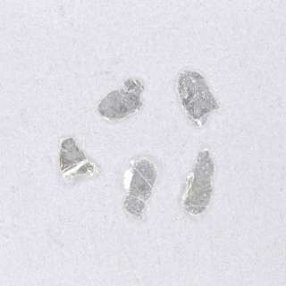 |
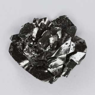
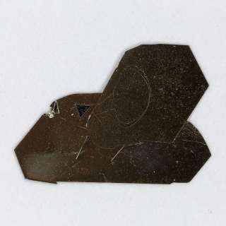
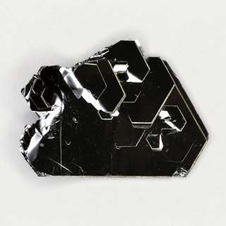
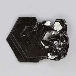
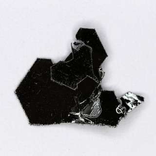
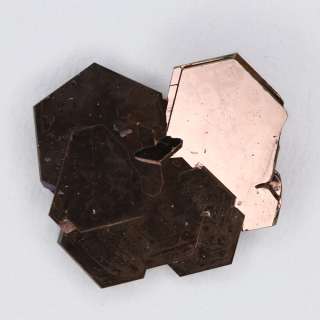
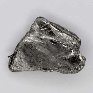
1.0-1.5mmのサイズで高純度(99.99%)の六方晶窒化ホウ素結晶は、科学研究に最適です。h-BN結晶状の単結晶グラフェンは、超高移動度を示します。また、非常に大きな降伏電圧(>0.4V/nm)で表される優れた絶縁体です。h-BN単結晶は、基板上(SiO2、ポリマー、石英等)で劈開することができ、劈開された結晶は、原子的に平坦で、原子力顕微鏡(AFM)下で非常に清潔な表面を示します。
h-BNは、グラファイトと同様に弱いファンデルワールス力による結合のため、簡単に劈開することができます。h-BN単層は、ホウ素と窒素原子間で共有結合により、非常に強く結合しています。空気中で1000℃、真空中で1400℃まで、優れた熱安定性を示します。
| 品名 |
結晶 |
サイズ |
純度 |
組成 |
数量 |
税別価格 |
型式 |
| 六方晶窒化ホウ素 |
Hexagonal |
1 mm |
>99.99% |
合成 |
20個 |
お問合せ |
BN2A1 |
|
|
【製品データ】
| 1. |
XRD:
X-ray diffraction on a hexagonal boron nitride single crystal aligned along
the (001) plane. XRD was performed at room temperature using a D8 Venture
Bruker. The 4 XRD peaks correspond, from left to right, to (001) with l
= 1, 2, 3 |
| 2. |
Raman:
Raman spectrum of a single crystal hexagonal boron nitride(h-BN). Measurement
was performed with a 785nm Raman system at room temperature. |
【論文及び参考文献】
|
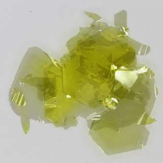 |
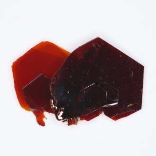
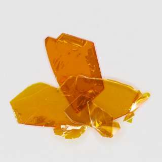
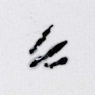
硫化ガリウムは、薄黄色の透明な結晶です。間接バンドを有する半導体です。結晶は、六方晶系の層状構造をしているため、簡単に劈開することができます。
| 品名 |
結晶 |
サイズ |
純度 |
組成 |
数量 |
税別価格 |
型式 |
| Gallium Sulfide |
Hexagonal |
6-8 mm |
>99.995% |
合成 |
1枚 |
お問合せ |
GaS |
|
|
【製品データ】
| 1. |
XRD:
X-ray diffraction on a GaS single crystal aligned along the (001) plane.
XRD was performed at room temperature using a D8 Venture Bruker. The 5
XRD peaks correspond, from left to right, to (001) with l = 2, 4, 6, 8,
10, 12, 14 |
| 2. |
XRD:
Powder X-ray diffraction(XRD) of a single crystal GaS. X-ray diffraction
was performed at room temperature using a D8 Venture Bruker. |
| 3. |
EDX:
Stoichiometric analysis of a single crystal alpha phase GaS by Energy-dispersive
X-ray spectroscopy(EDX). |
| 4. |
Raman:
Raman spectrum of a single crystal GaS. Measurement was performed with
a 785nm Raman system at room temperature. |
|
 |
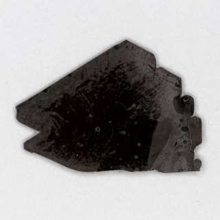
セレン化ガリウムは、茶色の結晶です。光学研究で使用され、間接バンドギャップを有する半導体です。層状構造は、ファンデルワールス力の結合のため、簡単に劈開することができます。
| 品名 |
結晶 |
サイズ |
純度 |
組成 |
数量 |
税別価格 |
型式 |
| Gallium Selenide |
Hexagonal |
6-8 mm |
>99.995% |
合成 |
1枚 |
お問合せ |
GaSe |
|
|
【製品データ】
| 1. |
XRD:
X-ray diffraction on a GaSe single crystal aligned along the (001) plane.
XRD was performed at room temperature using a D8 Venture Bruker. The 5
XRD peaks correspond, from left to right, to (001) with h = 4, 6, 8, 10,
12 |
| 2. |
XRD:
Powder X-ray diffraction(XRD) of a single crystal GaSe. X-ray diffraction
was performed at room temperature using a D8 Venture Bruker. |
| 3. |
EDX:
Stoichiometric analysis of a single crystal alpha phase GaSe by Energy-dispersive X-ray spectroscopy(EDX). |
| 4. |
Raman:
Raman spectrum of a single crystal GaSe. Measurement was performed with
a 785nm Raman system at room temperature. |
【論文及び参考文献】
|
 |
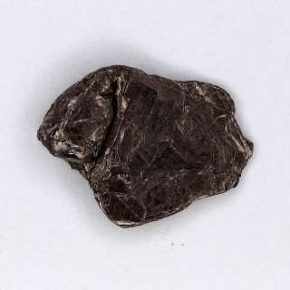
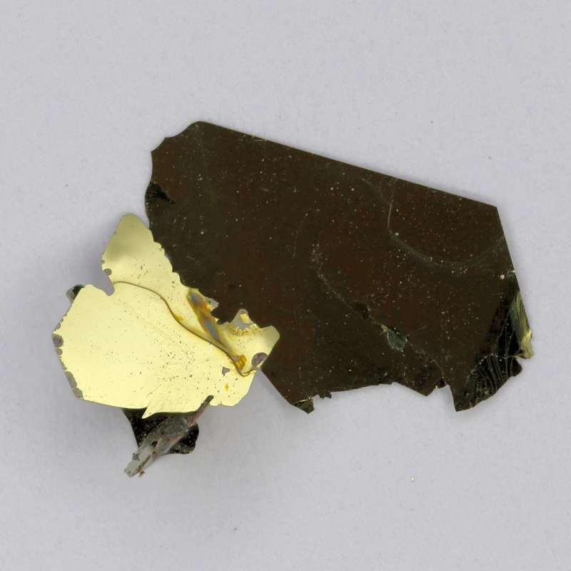
二硫化ハフニウムは、エンジ色の透明な結晶です。間接バンドを有する半導体です。結晶は層状構造をしているため、簡単に劈開することができます。
| 品名 |
結晶 |
サイズ |
純度 |
組成 |
数量 |
税別価格 |
型式 |
| Hafnium Sulfide |
Hexagonal |
6-8 mm |
>99.995% |
合成 |
1枚 |
お問合せ |
HfS2 |
|
|
【製品データ】
| 1. |
XRD:
X-ray diffraction on a HfS2 single crystal aligned along the (001) plane.
XRD was performed at room temperature using a D8 Venture Bruker. The 4
XRD peaks correspond, from left to right, to (001) with l = 1, 2, 3, 4 |
| 2. |
XRD:
Powder X-ray diffraction(XRD) of a single crystal HfS2. X-ray diffraction
was performed at room temperature using a D8 Venture Bruker. |
| 3. |
EDX:
Stoichiometric analysis of a single crystal HfS2 by Energy-dispersive X-ray
spectroscopy(EDX). |
| 4. |
Raman:
Raman spectrum of a single crystal HfS2. Measurement was performed with
a 785nm Raman system at room temperature. |
【論文及び参考文献】
|
 |
セレン化ハフニウムは、灰黒色の遷移金属ダイカルコゲナイトです。間接バンドギャップを有する半導体です。板状の結晶は層状構造で、ファンデルワールス力の結合のため、簡単に劈開することができます。
| 品名 |
結晶 |
サイズ |
純度 |
組成 |
数量 |
税別価格 |
型式 |
| Hafnium Selenide |
Hexagonal |
6-8 mm |
>99.995% |
合成 |
1枚 |
お問合せ |
HfSe2 |
|
|
【製品データ】
| 1. |
XRD:
X-ray diffraction on a Hafnium Diselenide single crystal aligned along
the (001) plane. XRD was performed at room temperature using a D8 Venture
Bruker. The 4 XRD peaks correspond, from left to right, to (001) with l
= 1, 3, 4, 5 |
| 2. |
XRD:
Powder X-ray diffraction(XRD) of a single crystal HfSe2. X-ray diffraction
was performed at room temperature using a D8 Venture Bruker. |
| 3. |
EDX:
Stoichiometric analysis of a single crystal HfSe2 by Energy-dispersive X-ray spectroscopy(EDX). |
| 4. |
Raman:
Raman spectrum of a single crystal HfSe2. Measurement was performed with
a 785nm Raman system at room temperature. |
【論文及び参考文献】
|
 |
| 品名 |
結晶 |
サイズ |
純度 |
組成 |
数量 |
税別価格 |
型式 |
| Indium Selenide |
Hexagonal |
6-8 mm |
>99.995% |
合成 |
1枚 |
お問合せ |
In2Se3(2H) |
|
|
【製品データ】
| 1. |
XRD:
X-ray diffraction on a 2H-In2Se3(Indium Selenide) single crystal aligned
along the (001) plane. XRD was performed at room temperature using a D8
Venture Bruker. The 8 XRD peaks correspond, from left to right, to (001)
with l = 4, 6, 8, 10, 12, 14, 16, 18 |
| 2. |
XRD:
Powder X-ray diffraction(XRD) of a single crystal In2Se3. X-ray diffraction
was performed at room temperature using a D8 Venture Bruker. |
| 3. |
EDX:
Stoichiometric analysis of a single crystal In2Se3 by Energy-dispersive
X-ray spectroscopy(EDX). |
|
 |
テルル化モリブデン黒色の結晶の遷移金属ダイカルコゲナイドです。関節バンドギャップを有する半導体です。結晶は層状構造で、ファンデルワールス力結合のため、簡単に劈開することができます。
| 品名 |
結晶 |
サイズ |
純度 |
組成 |
数量 |
税別価格 |
型式 |
| Molybdenum Ditelluride |
Hexagonal |
6-8 mm |
>99.995% |
合成 |
1枚 |
お問合せ |
MoTe2(2H) |
|
|
【製品データ】
| 1. |
XRD:
X-ray diffraction on a MoTe2 single crystal aligned along the (001) plane.
XRD was performed at room temperature using a D8 Venture Bruker. The 4
XRD peaks correspond, from left to right, to (001) with l = 2, 4, 6, 8 |
| 2. |
XRD:
Powder X-ray diffraction(XRD) of a single crystal MoTe2. X-ray diffraction
was performed at room temperature using a D8 Venture Bruker. |
| 3. |
EDX:
Stoichiometric analysis of a single crystal 2H MoTe2 by Energy-dispersive
X-ray spectroscopy(EDX). |
| 4. |
Raman:
Raman spectrum of a single crystal 2H MoTe2. Measurement was performed
with a 785nm Raman system at room temperature. |
|
 |
セレン化モリブデンは、直接バンドギャップを有する半導体です。層状構造は、ファンデルワールス力の結合で、遷移金属ダイカルコゲナイドです(TMDC)。トランジスタ、半導体の用途に使用可能です。
| 品名 |
結晶 |
サイズ |
純度 |
組成 |
数量 |
税別価格 |
型式 |
| Molybdenum Diselenide |
Hexagonal |
6-8 mm |
>99.995% |
合成 |
1枚 |
お問合せ |
MoSe2 |
|
|
【製品データ】
| 1. |
XRD:
X-ray diffraction on a MoSe2 single crystal aligned along the (001) plane.
XRD was performed at room temperature using a D8 Venture Bruker. The 4
XRD peaks correspond, from left to right, to (001) with l = 2, 4, 6, 8 |
| 2. |
XRD:
Powder X-ray diffraction(XRD) of a single crystal MoSe2. X-ray diffraction
was performed at room temperature using a D8 Venture Bruker. |
| 3. |
EDX:
Stoichiometric analysis of a single crystal MoSe2 by Energy-dispersive
X-ray spectroscopy(EDX). |
| 4. |
Raman:
Raman spectrum of a single crystal MoSe2. Measurement was performed with
a 785nm Raman system at room temperature. |
【論文及び参考文献】
| 1. |
Weigao Xu et al., "Correlated fluorescence blinking in two-dimensional
semiconductor heterostructures", Nature 541, 62-67(2017) |
| 2. |
Tomasz Jakubczyk et al., "Correlated fluorescence blinking in two-dimensional
semiconductor heterostructures", Nano Left., 2016, 16(9), pp 5333-5339 |
| 3. |
Beom Seo Kim et al., "Radiatively Limited Dephasing and Exciton Dynamics
in MoSe2 Monolayers Revealed with Four-Wave Mixing Microscopy", Nature/Scientific
Reports 6, Article number: 36389(2016) |
| 4. |
Kangwon Kim et al., "Davydov Splitting and Excitonic Resonance Effects
in Raman Spectra of Few-Layer MoSe2", ACS Nano 10, 8113-8120(2016) |
| 5. |
S. Dufferwiel et al., "Exciton-polaritons in van der Waals heterostructures
embedded in tunable microcavities", Nature Communications 6, 8579(2015) |
|
 |
二硫化レニウムは、銀黒色の遷移金属ダイカルコゲナイドです。間接バンドを有する半導体です。結晶は、個々の葉が花の様な層状構造になっています。ファンデルワールス力の結合のため、簡単に劈開することができます。
| 品名 |
結晶 |
サイズ |
純度 |
組成 |
数量 |
税別価格 |
型式 |
| Rhenium Sulfide |
Triclinic |
6-8 mm |
>99.995% |
合成 |
1枚 |
お問合せ |
ReS2 |
|
|
【製品データ】
| 1. |
XRD:
X-ray diffraction on a ReS2 single crystal aligned along the (001) plane.
XRD was performed at room temperature using a D8 Venture Bruker. The 5
XRD peaks correspond, from left to right, to (001) with l = 2, 4, 6, 8 |
| 2. |
XRD:
Powder X-ray diffraction(XRD) of a single crystal ReS2. X-ray diffraction
was performed at room temperature using a D8 Venture Bruker. |
| 3. |
EDX:
Stoichiometric analysis of a single crystal ReS2 by Energy-dispersive X-ray
spectroscopy(EDX). |
| 4. |
Raman:
Raman spectrum of a single crystal ReS2. Measurement was performed with
a 785nm Raman system at room temperature. |
【論文及び参考文献】
| 1. |
Sangwan Sim et al., "Selectively tunable optical Stark effect of anisotropic
excitons in stomically thin ReS2", ANat", Comm. 7:13569(2016) |
| 2. |
Daniel A. Chenet et al., "In-Plane Anisotropy in Mono- and Few-Layer
ReS2 Probed by Raman Spectroscopy and Scanning Transmission Electron Microscopy",
Nanoleft. 15(9), 5667-5672(2015) |
| 3. |
Ozgur Burak Asian et al., "Linearly Polarized Excitons in Single-
and Few-Layer ReS2 Crystals", ACS Photonics, 2016, 3(1), pp 96-101 |
|
 |
セレン化レニウムは、黒色の結晶の遷移金属ダイカルコゲナイドです。間接バンドギャップを有する半導体です。板状の結晶は層状構造で、ファンデルワールス力の結合のため、簡単に劈開することができます。
| 品名 |
結晶 |
サイズ |
純度 |
組成 |
数量 |
税別価格 |
型式 |
| Rhenium Selenide |
Triclinic |
6-8 mm |
>99.995% |
合成 |
1枚 |
お問合せ |
ReSe2 |
|
|
【製品データ】
| 1. |
XRD:
X-ray diffraction on a ReSe2 single crystal aligned along the (001) plane.
XRD was performed at room temperature using a D8 Venture Bruker. The 5
XRD peaks correspond, from left to right, to (001) with l = 1, 2, 3, 4,
5 |
| 2. |
XRD:
Powder X-ray diffraction(XRD) of a single crystal ReSe2. X-ray diffraction
was performed at room temperature using a D8 Venture Bruker. |
| 3. |
EDX:
Stoichiometric analysis of a single crystal ReSe2 by Energy-dispersive
X-ray spectroscopy(EDX). |
| 4. |
Raman:
Raman spectrum of a single crystal ReSe2. Measurement was performed with a 785nm Raman system at room temperature. |
【論文及び参考文献】
|
 |
二硫化スズは、橙黄色の遷移金属ダイカルコゲナイドです。間接バンドを有する半導体です。層状構造のため、簡単に劈開することができます。
| 品名 |
結晶 |
サイズ |
純度 |
組成 |
数量 |
税別価格 |
型式 |
| Tin Sulfide |
Hexagonal |
6-8 mm |
>99.995% |
合成 |
1枚 |
お問合せ |
SnS2 |
|
|
【製品データ】
| 1. |
XRD:
X-ray diffraction on a 2H phase Tin Disulfide aligned along the (001) plane.
XRD was performed at room temperature using a D8 Venture Bruker. The 4
XRD peaks correspond, from left to right, to (001) with l = 1, 2, 3, 4 |
| 2. |
XRD:
Powder X-ray diffraction(XRD) of a single crystal 2H-SnS2. X-ray diffraction
was performed at room temperature using a D8 Venture Bruker. |
| 3. |
EDX:
Stoichiometric analysis of a single crystal 2H-SnS2 by Energy-dispersive
X-ray spectroscopy(EDX). |
| 4. |
Raman:
Raman spectrum of a single crystal 2H-SnS2. Measurement was performed with
a 785nm Raman system at room temperature. |
|
 |
セレン化スズは、遷移金属ダイカルコゲナイドです。間接バンドギャップを有する半導体です。結晶は層状構造で、ファンデルワールス力の結合のため、簡単に劈開することができます。
| 品名 |
結晶 |
サイズ |
純度 |
組成 |
数量 |
税別価格 |
型式 |
| Tin Selenide |
Hexagonal |
6-8 mm |
>99.995% |
合成 |
1枚 |
お問合せ |
SnSe2 |
|
|
【製品データ】
| 1. |
XRD:
X-ray diffraction on a SnSe2 Single crystal aligned along the (001) plane.
XRD was performed at room temperature using a D8 Venture Bruker. The 5
XRD peaks correspond, from left to right, to (001) with l = 1, 2, 3, 4,
5 |
| 2. |
XRD:
Powder X-ray diffraction(XRD) of a single crystal SnSe2. X-ray diffraction
was performed at room temperature using a D8 Venture Bruker. |
| 3. |
EDX:
Stoichiometric analysis of a single crystal SnSe2 by Energy-dispersive X-ray spectroscopy(EDX). |
| 4. |
Raman:
Raman spectrum of a single crystal SnSe2. Measurement was performed with
a 785nm Raman system at room temperature. |
|
 |
二硫化タンタルは、黄黒色の遷移金属ダイカルコゲナイドです。最低温度相は、電荷密度波(CDW)上構造を有しています。層状構造は、ファンデルワールス力の結合のため、簡単に劈開することができます。
| 品名 |
結晶 |
サイズ |
純度 |
組成 |
数量 |
税別価格 |
型式 |
| Tantalum Sulfide |
Hexagonal |
6-8 mm |
>99.995% |
合成 |
1枚 |
お問合せ |
TaS2 (1T) |
|
|
【製品データ】
| 1. |
XRD:
X-ray diffraction on a Tantalum Disulfide single crystal aligned along
the (001) plane. XRD on the 1T-TaS2 was performed at room temperature using
a D8 Venture Bruker. The 5 XRD peaks correspond, from left to right, to
(001) with l = 1, 2, 3, 4, 5 |
| 2. |
XRD:
Powder X-ray diffraction(XRD) of a single crystal 1T-TaS2. X-ray diffraction
was performed at room temperature using a D8 Venture Bruker. |
| 3. |
EDX:
Stoichiometric analysis of a single crystal 1T-TaS2 by Energy-dispersive
X-ray spectroscopy(EDX). |
【論文及び参考文献】
|
 |
二硫化タングステンは、半導体です。室温のフォトルミネッセンスを示しています。水素とリチウムの貯蔵のための乾燥潤滑油として使用されています。
| 品名 |
結晶 |
サイズ |
純度 |
組成 |
数量 |
税別価格 |
型式 |
| Tungsten Disulfide |
Hexagonal |
6-8 mm |
>99.995% |
合成 |
1枚 |
お問合せ |
WS2 |
|
|
【製品データ】
| 1. |
XRD:
X-ray diffraction on a single crystal aligned along the (001) plane. XRD
was performed at room temperature using a D8 Venture Bruker. The 5 XRD
peaks correspond, from left to right, to (001) with l = 2, 4, 6, 8, 10 |
| 2. |
XRD:
Powder X-ray diffraction(XRD) of a single crystal 2H-WS2. X-ray diffraction
was performed at room temperature using a D8 Venture Bruker. |
| 3. |
EDX:
Stoichiometric analysis of a single crystal 2H-WS2 by Energy-dispersive
X-ray spectroscopy(EDX). |
| 4. |
Raman:
Raman spectrum of a single crystal 2H-WS2. Measurement was performed with
a 785nm Raman system at room temperature. |
【論文及び参考文献】
| 1. |
Humberto R. Guti rrez, et al. 'Extraordinary Room-Temperature Photoluminescence in Triangular WS2 Monolayers', Nano Lett., 2013, 13 (8), pp 3447 3454 |
| 2. |
Shaojun Wang et al., "Coherent Coupling of WS2 Monolayers with Metallic
Photonic Nanostructures at Room Temperature" Nano Lett. 16(7) |
| 3. |
Gerd Plechinger et al., "Excitonic valley effects in monolayer WS2
under high magnetic fields", Nano Lett., 2016, 16(12), pp 7899-7904 |
| 4. |
Beom Seo Kim et al., "Determination of the band parameters of bulk
2H-MX2(M=Mo, W; X=S, Se) by angle-resolved photoemission spectroscopy",
Nature/Scientific Reports 6, Article number: 36389(2016) |
|
 |
セレン化タングステンは、約1.35eVのバンドギャップを有する半導体です。層状構造でファンデルワールス力の結合です。6族遷移金属ダイカルコゲナイド(TMDC)です。
| 品名 |
結晶 |
サイズ |
純度 |
組成 |
数量 |
税別価格 |
型式 |
| Tungsten Diselenide |
Hexagonal |
6-8 mm |
>99.995% |
合成 |
1枚 |
お問合せ |
WSe2 |
|
|
【製品データ】
| 1. |
XRD:
X-ray diffraction on a WSe2 single crystal aligned along the (001) plane.
XRD was performed at room temperature using a D8 Venture Bruker. The 5
XRD peaks correspond, from left to right, to (001) with l = 2, 4, 6, 8,
10 |
| 2. |
XRD:
Powder X-ray diffraction(XRD) of a single crystal WSe2. X-ray diffraction
was performed at room temperature using a D8 Venture Bruker. |
| 3. |
EDX:
Stoichiometric analysis of a single crystal WSe2 by Energy-dispersive X-ray spectroscopy(EDX). |
| 4. |
Raman:
Raman spectrum of a single crystal WSe2. Measurement was performed with
a 785nm Raman system at room temperature. |
【論文及び参考文献】
| 1. |
H.C.P. Movva et al., "High-Mobility Holes in Dual-Gated WSe2 Field-Effect
Transistors", ACS Nano, 2015, 9(10), 10402-10410 |
| 2. |
B. Fallahazad et al., "Shubnikov-de Hass Oscillations of High-Mobility
Holes in Monolayer and Bilaver WSe2: Landau Level Degeneracy, Effective
Mass, and Negative Compressibility", Phys. Rev. Lett. 116, 086601(2016),
(also available on arxiv.org/pdf/1602.01073.pdf) |
| 3. |
R. Bertoni et al., "Generation and Evolution of Spin-, Valley-, and
Layer-Polarized Excited Carriers in Inversion- Symmetric WSe2", Phys.
Rev. Lett. 117, 277201(2016), (also available on arxiv. org/abs/1606.03218) |
|
◆その他製品ラインナップ
|
| As2Te3 |
Bi2S3 |
GaTe |
GeS |
GeSe |
MoS2 |
MoWSe2 |
| MoW2 |
Pb5Sn3Sb2S14 |
PbSnS2 |
P-As |
Sb2Te3 |
ZrSe2 |
ZrTe3 |
|
|
 金属 金属
|
 |
| 品名 |
グレード |
結晶 |
サイズ |
純度 |
組成 |
数量 |
税別価格 |
型式 |
| グラフェン結晶 |
ZYA |
Hexagonal |
12×12 mm |
>99.995% |
合成 |
1枚 |
お問合せ |
HOPG-ZYA |
| ZYB |
HOPG-ZYB |
|
|
【製品データ】
| 1. |
XRD:
X-ray diffraction on a HOPG single crystal aligned along the (001) plane.
XRD was performed at room temperature using a D8 Venture Bruker. The 3
XRD peaks correspond, from left to right, to (001) with l = 1, 2, 3 |
|
 |
セレン化ニオブは、灰黒色の結晶の遷移金属ダイカルコゲナイドです。30K以上で電荷密度波遷移を示すことが報告されており、Tcは約7.2Kの超伝導体です。結晶は層状構造でファンデルワールス力の結合のため、簡単に劈開することができます。
| 品名 |
結晶 |
サイズ |
純度 |
組成 |
数量 |
税別価格 |
型式 |
| Niobium Selenide |
Hexagonal |
6-8 mm |
>99.995% |
合成 |
1枚 |
お問合せ |
2H-NbSe2 |
|
|
【製品データ】
| 1. |
XRD:
X-ray diffraction on a 2H phase NbSe2 single crystal aligned along the
(001) plane. XRD was performed at room temperature using a D8 Venture Bruker.
The 4 XRD peaks correspond, from left to right, to (001) with l = 2, 4,
6, 8 |
| 2. |
XRD:
Powder X-ray diffraction(XRD) of a single crystal 2H NbSe2. X-ray diffraction
was performed at room temperature using a D8 Venture Bruker. |
| 3. |
EDX:
Stoichiometric analysis of a single crystal 2H NbSe2 by Energy-dispersive
X-ray spectroscopy(EDX). |
| 4. |
Raman:
Raman spectrum of a single crystal 2H NbSe2. Measurement was performed
with a 785nm Raman system at room temperature. |
【論文及び参考文献】
|
 |
二硫化ニオブは、Tc(転移温度)が約6Kの超伝導体です。結晶は、灰から黒色の外観、層状構造のため、簡単に劈開することができます。
| 品名 |
結晶 |
サイズ |
純度 |
組成 |
数量 |
税別価格 |
型式 |
| Niobium Sulfide |
Hexagonal |
1.5-2 mm |
>99.995% |
合成 |
1枚 |
お問合せ |
NbS2(2H) |
|
|
【製品データ】
| 1. |
XRD:
X-ray diffraction on a Single crystal 2H-NbS2 aligned along the (001) plane.
XRD diffraction was performed at room temperature using a D8 Venture Bruker.
The 4 XRD peaks correspond, from left to right, to (001) with l = 2, 4,
6, 8 |
| 2. |
XRD:
Powder X-ray diffraction(XRD) of a single crystal 2H-NbS2. X-ray diffraction
was performed at room temperature using a D8 Venture Bruker. |
|
 |
セレン化バナジウムは、遷移金属ダイカルコゲナイドです。結晶は層状構造でファンデルワールス力の結合のため、簡単に劈開することができます。
| 品名 |
結晶 |
サイズ |
純度 |
組成 |
数量 |
税別価格 |
型式 |
| Vanadium Diselenide |
Hexagonal |
6-8 mm |
>99.995% |
合成 |
1枚 |
お問合せ |
VSe2(1T) |
|
|
【製品データ】
| 1. |
XRD:
X-ray diffraction on a Vanadium Diselenide single crystal aligned along
the (001) plane. XRD was performed at room temperature using a D8 Venture
Bruker. The 4 XRD peaks correspond, from left to right, to (001) with l
= 1, 2, 3, 4 |
| 2. |
XRD:
Powder X-ray diffraction(XRD) of a single crystal VSe2. X-ray diffraction
was performed at room temperature using a D8 Venture Bruker. |
| 3. |
EDX:
Stoichiometric analysis of a single crystal VSe2 by Energy-dispersive X-ray
spectroscopy(EDX). |
| 4. |
Raman:
Raman spectrum of a single crystal VSe2. Measurement was performed with
a 785nm Raman system at room temperature. |
|
|
 半金属 半金属
|
 |
二硫化チタンは、金色の遷移金属ダイカルコゲナイトです。半金属であり、二次電池などの正極材料として使用することができます。層状構造は、ファンデルワールス力の結合のため、簡単に劈開することができます。
| 品名 |
結晶 |
サイズ |
純度 |
組成 |
数量 |
税別価格 |
型式 |
| Titanium Sulfide |
Hexagonal |
6-8 mm |
>99.995% |
合成 |
1枚 |
お問合せ |
TiS2(1T) |
|
|
【製品データ】
| 1. |
XRD:
X-ray diffraction on a TiS2 single crystal aligned along the (001) plane.
XRD was performed at room temperature using a D8 Venture Bruker. The 4
XRD peaks correspond, from left to right, to (001) with l = 1, 2, 3, 4 |
| 2. |
XRD:
Powder X-ray diffraction(XRD) of a single crystal TiS2. X-ray diffraction
was performed at room temperature using a D8 Venture Bruker. |
| 3. |
EDX:
Stoichiometric analysis of a single crystal TiS2 by Energy-dispersive X-ray
spectroscopy(EDX). |
| 4. |
Raman:
Raman spectrum of a single crystal TiS2. Measurement was performed with
a 785nm Raman system at room temperature. |
|
 |
セレン化チタンは、銅-黒色の結晶の遷移金属ダイカルコゲナイドです。半導体または半金属であると考えられます。板状の結晶は層状構造でファンデルワールス力の結合のため、簡単に劈開することができます。
| 品名 |
結晶 |
サイズ |
純度 |
組成 |
数量 |
税別価格 |
型式 |
| Titanium Selenide |
Hexagonal |
6-8 mm |
>99.995% |
合成 |
1枚 |
お問合せ |
TiSe2 |
|
|
【製品データ】
| 1. |
XRD:
X-ray diffraction on a TiSe2 single crystal aligned along the (001) plane. XRD was performed at room temperature using a D8 Venture Bruker. The 4 XRD peaks correspond, from left to right, to (001) with l = 1, 2, 3, 4 |
| 2. |
XRD:
Powder X-ray diffraction(XRD) of a single crystal TiSe2. X-ray diffraction
was performed at room temperature using a D8 Venture Bruker. |
| 3. |
EDX:
Stoichiometric analysis of a single crystal TiSe2 by Energy-dispersive
X-ray spectroscopy(EDX). |
| 4. |
Raman:
Raman spectrum of a single crystal TiSe2. Measurement was performed with a 785nm Raman system at room temperature. |
|
 |
テルル化タングステンは半導体です。6族遷移金属ダイカルコゲナイド(TMDC)です。結晶は層状構造で、ファンデルワールス力結合です。
| 品名 |
結晶 |
サイズ |
純度 |
組成 |
数量 |
税別価格 |
型式 |
| Tungsten Ditelluride |
orthorhombic |
- |
>99.995% |
合成 |
1枚 |
お問合せ |
WTe2 |
|
|
【製品データ】
| 1. |
XRD:
X-ray diffraction on a WTe2 single crystal aligned along the (001) plane.
XRD was performed at room temperature using a D8 Venture Bruker. The 5
XRD peaks correspond, from left to right, to (001) with l = 2, 4, 6, 8,
10 |
| 2. |
XRD:
Powder X-ray diffraction(XRD) of a single crystal WTe2. X-ray diffraction
was performed at room temperature using a D8 Venture Bruker. |
| 3. |
EDX:
Stoichiometric analysis of a single crystal WTe2 by Energy-dispersive X-ray
spectroscopy(EDX). |
| 4. |
Raman:
Raman spectrum of a single crystal WTe2. Measurement was performed with
a 785nm Raman system at room temperature. |
【論文及び参考文献】
|
|
 超電導体 超電導体
|
 |
セレン化タンタル黒色の遷移金属ダイカルコゲナイトです。結晶は層状構造で、ファンデルワールス力の結合のため、簡単に劈開することができます。
| 品名 |
結晶 |
サイズ |
純度 |
組成 |
数量 |
税別価格 |
型式 |
| Tantalum Selenide |
Hexagonal |
6-8 mm |
>99.995% |
合成 |
1枚 |
お問合せ |
TaSe2(2H) |
|
|
【製品データ】
| 1. |
XRD:
X-ray diffraction on a 2H-TaSe2 single crystal aligned along the (001)
plane. XRD was performed at room temperature using a D8 Venture Bruker.
The 4 XRD peaks correspond, from left to right, to (001) with l = 2, 6,
8, 10 |
| 2. |
XRD:
Powder X-ray diffraction(XRD) of a single crystal 2H-TaSe2. X-ray diffraction
was performed at room temperature using a D8 Venture Bruker. |
| 3. |
EDX:
Stoichiometric analysis of a single crystal 2H-TaSe2 by Energy-dispersive
X-ray spectroscopy(EDX). |
| 4. |
Raman:
Raman spectrum of a single crystal 2H-TaSe2. Measurement was performed
with a 785nm Raman system at room temperature. |
|
|
トポロジカル絶縁体
|
 |
セレン化ビスマスは、黒灰色の結晶のトポロジカル絶縁体です。層状構造は、ファンデルワールス力の結合のため、簡単に劈開することができます。
参考文献:
| 品名 |
結晶 |
サイズ |
純度 |
組成 |
数量 |
税別価格 |
型式 |
| Bismuth Selenide |
Rhombohedral |
6-8 mm |
>99.995% |
合成 |
1枚 |
お問合せ |
Bi2Se3 |
|
|
【製品データ】
| 1. |
XRD:
X-ray diffraction on a Bi2Se3 single crystal aligned along the (001) plane.
XRD was performed at room temperature using a D8 Venture Bruker. The 6
XRD peaks correspond, from left to right, to (001) with l = 6, 9, 12, 15,
18, 21, 24 |
| 2. |
XRD:
Powder X-ray diffraction(XRD) of a single crystal Bi2Se3. X-ray diffraction
was performed at room temperature using a D8 Venture Bruker. |
| 3. |
EDX:
Stoichiometric analysis of a single crystal Bi2Se3 by Energy-dispersive
X-ray spectroscopy(EDX). |
| 4. |
Raman:
Raman spectrum of a single crystal Bi2Se3. Measurement was performed with
a 785nm Raman system at room temperature. |
【論文及び参考文献】
|
 |
テルル化ビスマスは、トポロジカル絶縁体です。結晶は、層状構造で、ファンデルワールス力結合のため、簡単に劈開することができます。
| 品名 |
結晶 |
サイズ |
純度 |
組成 |
数量 |
税別価格 |
型式 |
| Bismuth Telluride |
Rhombohedral |
6-8 mm |
>99.995% |
合成 |
1枚 |
お問合せ |
Bi2Te3 |
|
|
【製品データ】
| 1. |
XRD:
X-ray diffraction on a Bi2Te3 single crystal aligned along the (001) plane.
XRD was performed at room temperature using a D8 Venture Bruker. |
| 2. |
EDX:
Stoichiometric analysis of a single crystal Bi2Te3 by Energy-dispersive
X-ray spectroscopy(EDX). |
|
|
|